615 GHz Set A Record! New High Speed Germanium Silicon Avalanche Photodetector
Recently, the team of Professor Daozin Dai from the School of Optoelectronic Science and Engineering of Zhejiang University proposed a silicon germanium avalanche photodetector that a standard tape-out process can fabricate.
The device has superior performance, achieving a record gain-bandwidth product GBP of up to 615 GHz. It successfully demonstrated its 100 Gbps NRZ and PAM-4 high-speed signal reception, laying the core optical device foundation for next-generation high-speed silicon photonics integrated optical reception, which has important application prospects.
The related research results were published on Optica on July 5, 2022, under the title “High-speed waveguide Ge/Si avalanche photodiode with a record gain-bandwidth product of 615 GHz”.
Research Background
With the rise of new services such as cloud services, artificial intelligence, and the Internet of Things, the data transmission rate and capacity are facing unprecedented challenges, and the key lies in the development of high-speed optoelectronic devices. In the past 10 years, silicon-based optoelectronics has developed rapidly. It has become an emerging mainstream technology in integrated optoelectronics with outstanding advantages, such as CMOS compatibility and high integration. How to achieve higher performance to meet the needs of next-generation applications is an important issue facing its current development. challenge.
As we all know, high-performance photodetectors are indispensable core devices for almost all optical systems. To obtain higher sensitivity, avalanche photodetectors (APDs) with internal gains, such as germanium-silicon APDs, have been developed. The previously reported SiGe APDs have a low gain-bandwidth product (usually ~300 GHz). They often require the introduction of complex multiple epitaxial vertical structures or fine local doping structures, which are difficult to meet the development needs of future high-speed and high-sensitivity receivers.
Research innovation
In response to this problem, the team recently reported the latest research results of germanium-silicon APD with ultra-high gain-bandwidth products. Based on the 180 nm standard tape-out process, they proposed and implemented a lateral pull-through silicon-germanium waveguide APD with the ultra-high gain-bandwidth product, as shown in the figure below.
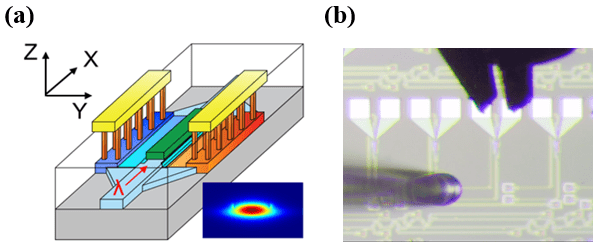
In this device, through the non-uniformization of the electric field in the silicon multiplication region, the “dead space” effect is cleverly used to reduce further the equivalent ionization ratio of the silicon multiplication region, effectively reducing its excess noise and break through its gain-bandwidth product GBP restriction. At the same time, the shallow-etched ridge waveguide structure design is innovatively introduced, which realizes beneficial regulation of the optical field and electric field of the device.
On the one hand, it helps to enhance the light absorption rate of the germanium region, thereby improving its responsivity; on the other hand, it effectively suppresses the fringe electric field strength of the germanium region, which helps to reduce the APD dark current. What is particularly important is that the APD only needs to use a standard CMOS single-shot germanium epitaxy process, avoiding complex processes such as multiple epitaxy required by the traditional vertical separation absorption charge multiplying structure APD.
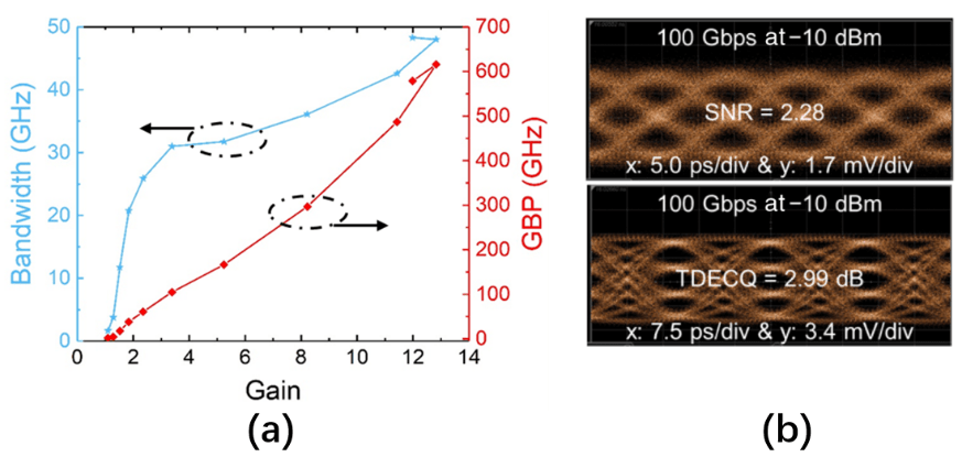
The APD device developed by the team operates in the O-band (as shown in Figure 2), with an operating voltage of about −14 V and a unity-gain responsivity of 0.93 A/W. In particular, the device achieves a 48 GHz bandwidth with a gain factor as high as 12.8, corresponding to a gain-bandwidth product as high as 615 GHz, as shown in Figure 2a. Based on this APD, the research team conducted high-speed signal reception experiments. It successfully demonstrated the reception of NRZ and PAM-4 signals up to 100 Gbps, as shown in Figure 2b, with sensitivities of −12.6 dBm and −11.3 dBm, respectively (BER= 2.4×10⁻⁴).
The research results show that the APD device successfully developed in this work has superior performance and a simple process and has broad application potential.
Summary and Outlook
The high-performance APD device developed by the team has laid a key foundation for the high-sensitivity reception of high-speed optical signals. The process is simple and compatible with core functional device processes such as passive silicon optical devices and optical modulators, which can further build multi-functional integrated applications. with broad application foreground.


