Advances In Two Dimensional Material Photodetectors In China
The study of two-dimensional materials began with the discovery of graphene. After more than ten years of rapid development, the research on electronic and optoelectronic devices based on two-dimensional materials has achieved a series of striking results. Among them, new structures with excellent optoelectronic properties have been continuously designed and fabricated, which has rapidly promoted the development of two-dimensional material photodetectors.

A series of high-performance photodetectors have been reported one after another. For example, ultra-broadband two-dimensional material photodetectors can achieve high-sensitivity detection from ultraviolet to infrared and even terahertz bands.
The ultra-fast response speed of graphene detectors has a bandwidth higher than 100 GHz, some mid- and long-wave infrared detectors based on two-dimensional material heterojunctions have achieved room-temperature operation. In addition, large-area array high-sensitivity near-infrared focal plane devices have also been successfully developed, and an array imaging of 388´288 has been achieved (Nat. Photon., 2017, 11, 366), and it is gradually developing towards practicality.
In terms of photodetection, traditional thin-film semiconductors (such as Si, GaN, InGaAs, InSb, HgCdTe, etc.) have always dominated the market. The next-generation photodetectors are developing in the direction of room temperature, broadband, ultra-sensitive, ultra-small pixels, ultra-large area arrays, and multi-dimensional optical information detection. The development of new two-dimensional material photodetectors and their heterostructure detectors has ushered in new opportunities and challenges. Compared with traditional three-dimensional thin-film semiconductors, the size of two-dimensional materials in one dimension is much smaller than the wavelength of light, which can achieve lower dark current and noise.
However, two-dimensional materials with a thick atomic layer have high light transmittance, and light absorption is not as good as that of thin-film materials. How to realize the interaction of super-strong light and matter, and how to realize infrared detection at room temperature? What is the physical mechanism that enables superior photodetection performance on such thin materials? Are there any insurmountable shortcomings? What is the future direction of development? The working mechanism and application value of such devices are worth exploring and summarizing.
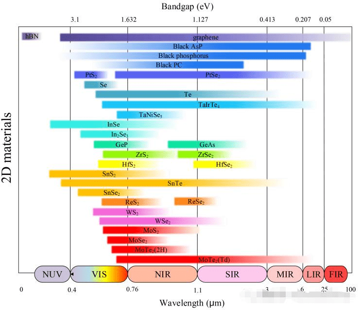
At present, two-dimensional material detectors can achieve ultra-high single-performance indicators, such as photoresponsivity up to ~10^10 A/W, photoconductive gain ~10^12, frequency response ~128 GHz, response time ~1 ps, etc. However, the practical application of the device needs to consider the comprehensive performance and development cost of the device.
Ultra-high optical gain based on the Photogating effect comes at the expense of response time. Most graphene detectors can achieve fast photoresponse, but the responsivity is very low. The key issues that need to be solved at present are how to achieve high sensitivity and fast detection at the same time, and how to suppress dark currents and noise without losing the responsivity of the device. In addition, how to achieve large-area preparation of two-dimensional materials, promote the development of unit devices to large-scale area arrays, and realize the upgrade from single light intensity detection to multi-dimensional light information detection is also a serious challenge.
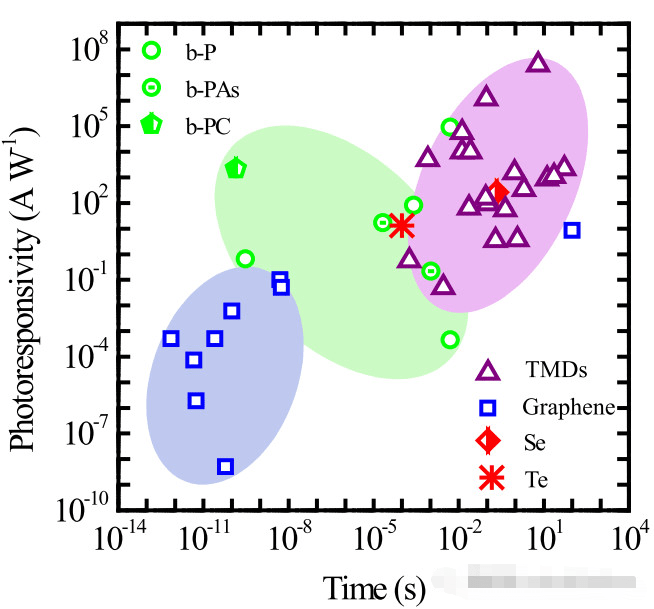
Graphene detectors are mainly suitable for fast photodetection, but the responsivity is low; transition metal chalcogenides have high responsivity, but the relative response time is long; the photoresponsivity and response speed of black phosphorus is between the two. Therefore, black phosphorus is an important material that can achieve a high response rate and response speed at the same time. Currently, only black phosphorus achieves direct blackbody response in two-dimensional material detectors, and the response band is in the mid-wave infrared.
Further narrowing the bandgap of black phosphorus materials and exploring new two-dimensional narrow-band materials are important ways to realize the practical application of room temperature mid- and long-wave infrared detection based on two-dimensional materials. In addition, the large-scale preparation of two-dimensional materials is also an important area that needs to be developed.
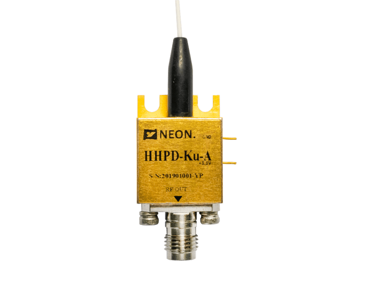
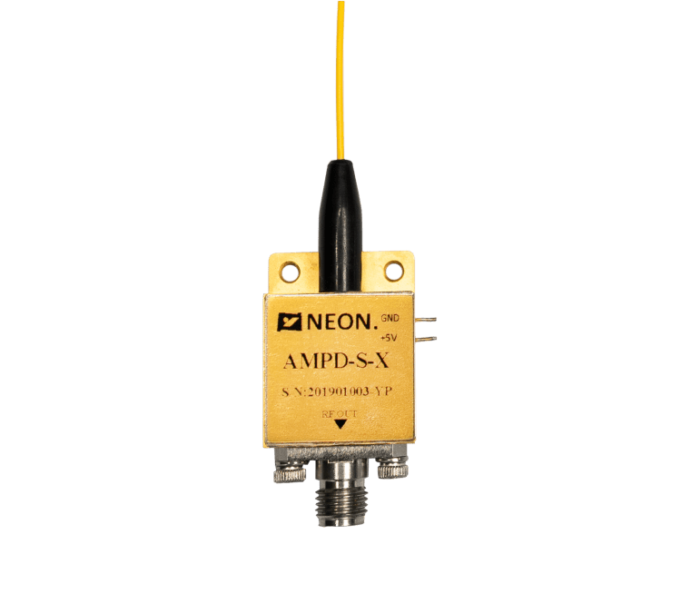
As a supplier of high-quality photodetectors in China, NEON has advanced InGaAs photodetector technology. If you need any help, you can contact us, and we will provide you with a photodetector suitable for you.


