New Technology! New High-Performance Photodetectors For Silicon Photonics
As data communications and data traffic continue to grow, traditional electronic interconnections are reaching their limits. Silicon (Si) photonics has become the preferred technology to solve this problem due to its advantages of high speed, large bandwidth, low cost, high energy efficiency, and scalable manufacturing.
In this technology, fast, high-performance photodetectors are undoubtedly a key element. To operate effectively in data interconnection, such integrated photodetectors need to have a broadband operation, high responsivity, and low “dark current” performance on the one hand, and also need to cooperate with existing CMOS manufacturing systems, especially It is effectively coupled to the optical waveguide on silicon.

In this context, researchers began to look for new material systems to try to meet the target requirements. At present, this new material system is mainly divided into two types: one is germanium-based materials, which are generally compatible with silicon and operate at telecommunication wavelengths. It has a large bandwidth and good responsivity, but this material is prone to lattice mismatch, resulting in crystal defects or dislocations, resulting in high dark current and reduced sensitivity; the second is group III-V materials, which can be used in, However, their low optical coupling efficiency with silicon in practical devices hinders their further development.
To address these issues, Keu May Lau et al. of the Hong Kong University of Science and Technology cleverly combined several micropatterned structures and deposition techniques to create a monolithic indium phosphate/silicon-on-insulator (InP/SOI) platform and High-performance photodetectors made of III-V materials are grown on this platform, and the related results have been published in Optica.
The preparation method of this platform is mainly divided into the following four steps:
(1) Patterning the 480 nm thick Si layer on the SOI wafer into Si segments with the same width and different lengths;
(2) Encapsulation with a thin oxide layer above the Si layer;
(3) Use a wet etching process to remove Si in selected areas below the top oxide layer and leave a gap between the oxide and the bottom insulating oxide layer;
(4) InP is filled in the gap by lateral epitaxial growth technology to generate an “InP-on-insulator” structure with SOI.
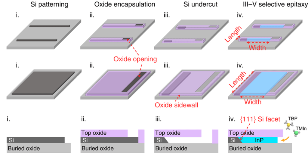
The InP structure layer of this structure can be coplanar with the Si device layer, not only for efficient optical coupling with silicon waveguides but also for high-speed photodetection using InP or other III-V materials.
To demonstrate this conclusion, the researchers fabricated photodetectors of various detectors and configurations using sequences of InP and InGaAs materials on monolithic InP/SOI substrates and tested 3 dB bandwidths with high bandwidths (over 40 GHz). ), high responsivity, wide operating wavelength, and low dark current (0.55 nA) meet all the criteria required for high-performance photodetectors in data communications.
Its researchers say the photodetectors they developed based on the new deposition process are “qualified candidates for future data communications in silicon photonics” and that the capabilities enabled by the on-chip lasers on this platform are more promising for fully integrated silicon photonics.


