The Difference Between Different Types of Photodetectors
This tutorial focuses on reverse-biased p-n junctions that are commonly used for making optical receivers. Metal-semiconductor-metal (MSM) photodetectors are also discussed briefly.
1. P-N PHOTODIODES
A reverse-biased p-n junction consists of a region, known as the depletion region, that is essentially devoid of free charge carriers and where a large built-in electric field opposes the flow of electrons from the n-side to the p-side (and of holes from p to n).
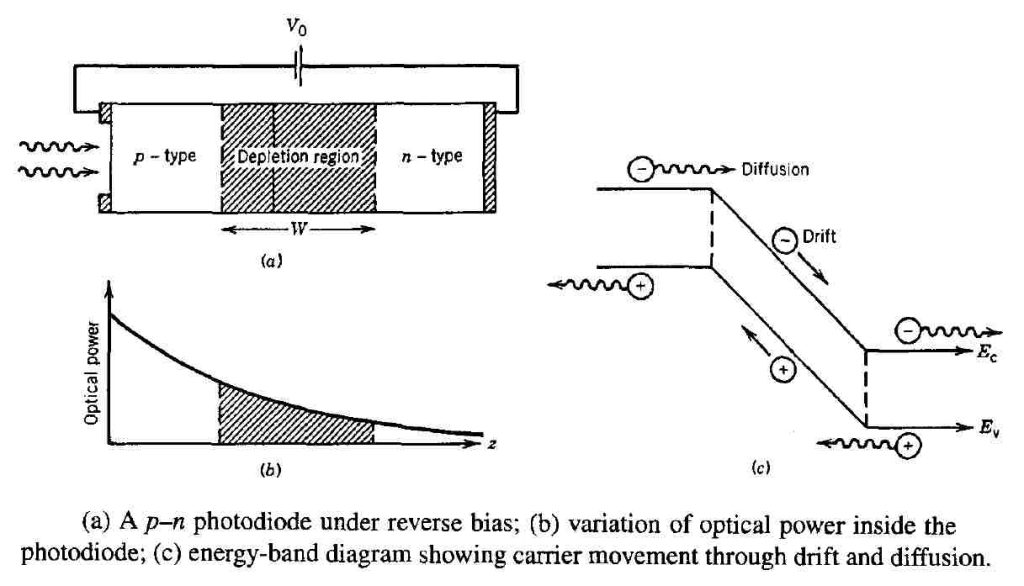
When such a p-n junction is illuminated with light on one side, say the p-side, electron-hole pairs are created through absorption. Because of the large built-in electric field, electrons and holes generated inside the depletion region accelerate in opposite directions and drift to the n- and p-sides, respectively. The resulting flow of current is proportional to the incident optical power. Thus a reverse-biased p-n junction acts as a photodetector and is referred to as the p-n photodiode.
Figure (a) above shows the structure of a p-n photodiode. As shown in (b), optical power decreases exponentially as the incident light is absorbed inside the depletion region. The electron-hole pairs generated inside the depletion region experience a large electric field and drift rapidly toward the p- or n-side, depending on the electric charge (figure (c)). The resulting current flow constitutes the photodiode response to the incident optical power in accordance with the equation we derived earlier. The responsivity of a photodiode is quite high (R ~ 1 A/W) because of its high quantum efficiency.
The bandwidth of a p-n photodiode is often limited by the transit time τtr. If W is the width of the depletion region and vd is the drift velocity, the transit time is given by
τtr = W/vd
Typically, W ~10 μm, vd ~ 105 m/s, and τtr ~ 100 ps. Both W and vd can be optimized to minimize τtr. The depletion-layer width depends on the acceptor and donor concentrations and can be controlled through them. The velocity vd depends on the applied voltage but attains a maximum value (called the saturation velocity) ~ 105 m/s that depends on the material used for the photodiode. The RC time constant τRC can be written as
τRC = (RL + RS)Cp
where RL is the external load resistance, RS is the internal series resistance, and Cp is the parasitic capacitance. Typically, τRC ~ 100 ps, although lower values are possible with a proper design. Indeed, modern p-n photodiodes are capable of operating at bit rates of up to 40 Gb/s.
The limiting factor for the bandwidth of p-n photodiodes is the presence of a diffusive component in the photocurrent. The physical origin of the diffusive component is related to the absorption of incident light outside the depletion region. Electrons generated in the p-region have to diffuse to the depletion-region boundary before they can drift to the n-side; similarly, holes generated in the n-region must diffuse to the depletion-region boundary. Diffusion is an inherently slow process; carriers take a nanosecond or longer to diffuse over a distance of 1 μm. The following figure shows how the presence of a diffusive component can distort the temporal response of a photodiode.
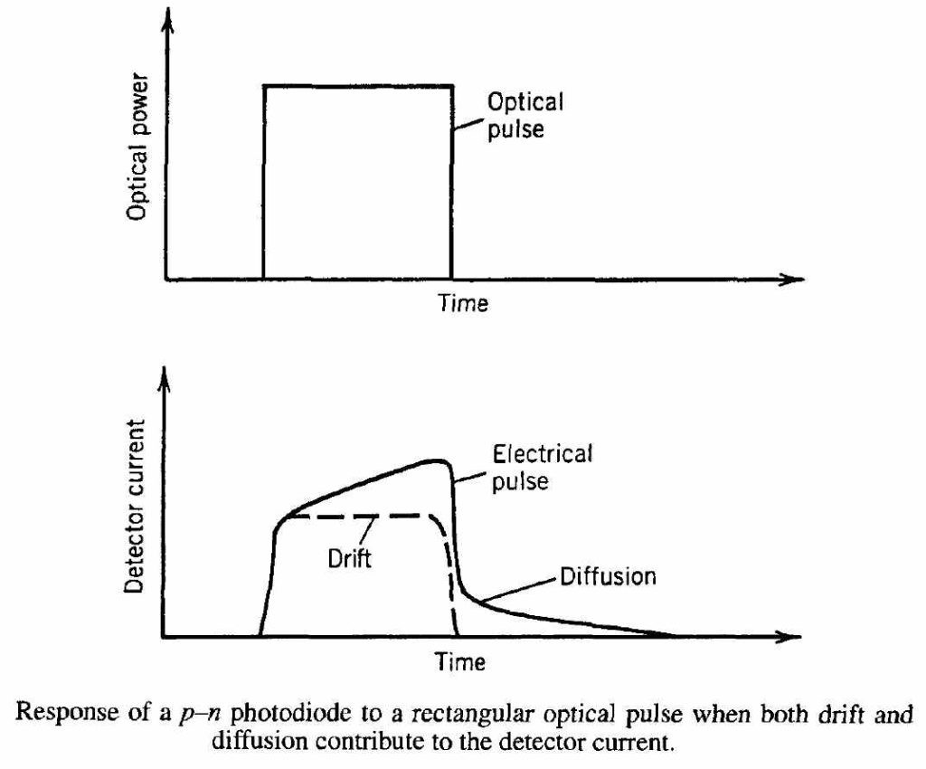
The diffusion contribution can be reduced by decreasing the widths of the p- and n-regions and increasing the depletion-region width so that most of the incident optical power is absorbed inside it. This is the approach adopted for p-i-n photodiodes, discussed next.
2. P-I-N PHOTODIODES
A simple way to increase the depletion-region width is to insert a layer of undoped (or lightly doped) semiconductor material between the p-n junction. Since the middle layer consists of nearly intrinsic material, such a structure is referred to as the p-i-n photodiode. Figure (a) below shows the device structure together with the electric-field distribution inside it under reverse-bias operation.
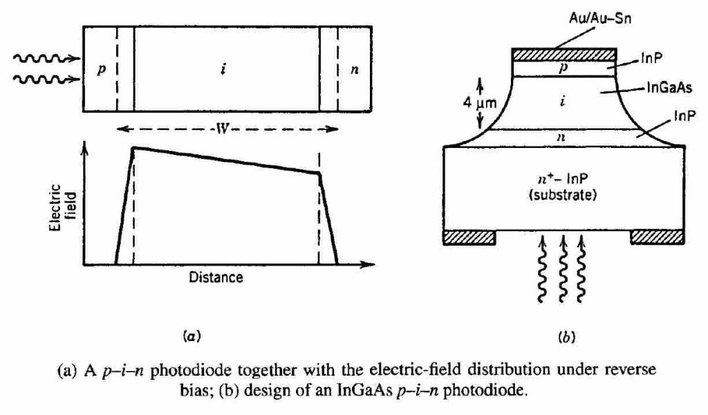
Because of its intrinsic nature, the middle i-layer offers high resistance, and most of the voltage drop occurs across it. As a result, a large electric field exists in the i-layer. In essence, the depletion region extends throughout the i-region, and its width W can be controlled by changing the middle-layer thickness. The main difference from the p-n photodiode is that the drift component of photocurrent dominates over the diffusion component simply because most of the incident power is absorbed inside the i-region of a p-i-n photodiode.
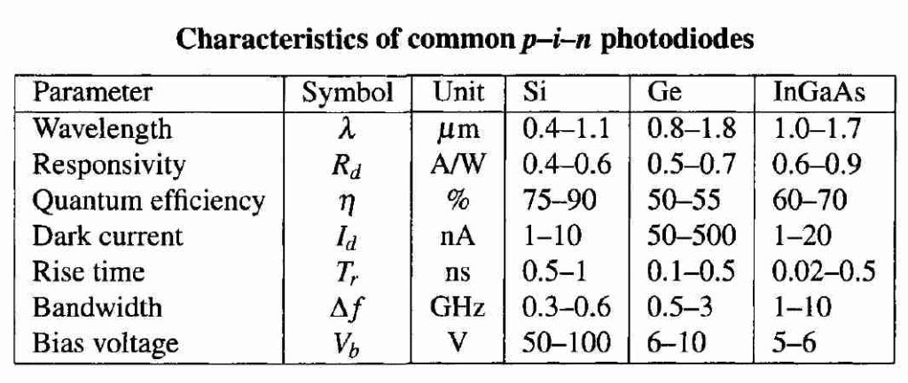
Since the depletion width W can be tailored in p-i-n photodiodes, a natural question is how large W should be. As discussed before, the optimum value of W depends on a compromise between speed and sensitivity. The responsivity can be increased by increasing W so that the quantum efficiency η approaches 100%. However, the response time also increases, as it takes longer for carriers to drift across the depletion region. For indirect-bandgap semiconductors such as Si and Ge, typically W must be in the range of 20-50 μm to ensure a reasonable quantum efficiency. The bandwidth of such photodiodes is then limited by a relatively long transit time (τtr > 200 ps). By contrast, W can be as small as 3-5 μm for photodiodes that use direct-bandgap semiconductors, such as InGaAs. The transit time for such photodiodes is τtr ~ 10 ps. Such values of τtr correspond to a detector bandwidth Δf ~ 10 GHz with τtr >> τRC.
The performance of p-i-n photodiodes can be improved considerably by using a double-heterostructure design. Similar to the case of semiconductor lasers, the middle i-type layer is sandwiched between the p-type and n-type layers of a different semiconductor whose bandgap is chosen such that light is absorbed only in the middle i-layer.
A p-i-n photodiode commonly used for lightwave applications uses InGaAs for the middle layer and InP for the surrounding p-type and n-type layers. Figure (b) above shows such an InGaAs p-i-n photodiode. Since the bandgap of InP is 1.35 eV, InP is transparent for light whose wavelength exceeds 0.92 μm. By contrast, the bandgap of lattice-matched In1-xGaxAs material with x = 0.47 is about 0.75 eV, a value that corresponds to a cutoff wavelength of 1.65 μm. The middle InGaAs layer thus absorbs strongly in the wavelength region 1.3-1.6 μm.
The diffusive component of the detector current is eliminated completely in such a heterostructure photodiode simply because photons are absorbed only inside the depletion region. The front facet is often coated using suitable dielectric layers to minimize reflections. The quantum efficiency η can be made almost 100% by using an InGaAs layer 4-5 μm thick. InGaAs photodiodes are quite useful for lightwave systems and are often used in practice. The table below lists the operating characteristics of three common p-i-n photodiodes.
Considerable effort was directed during the 1990s toward developing high-speed p-i-n photodiodes capable of operating at bit rates exceeding 10 Gb/s. Bandwidths of up to 70 GHz were realized as early as 1986 by using a thin absorption layer (< 1 μm) and by reducing the parasitic capacitance Cp with a small size, but only at the expense of lower quantum efficiency and responsivity. By 1995, p-i-n photodiodes exhibited a bandwidth of 110 GHz for devices designed to reduce τRC to near 1 ps.
Several techniques have been developed to improve the efficiency of high-speed photodiodes. In one approach, a Fabry-Perot (FP) cavity is formed around the p-i-n structure to enhance the quantum efficiency, resulting in a laser-like structure. As discussed before, an FP cavity has a set of longitudinal modes at which the internal optical field is resonantly enhanced through constructive interference. As a result, when the incident wavelength is close to a longitudinal mode, such a photodiode exhibits high sensitivity.
The wavelength selectivity can be used to advantage in wavelength-division multiplexing (WDM) applications. A nearly 100% quantum efficiency was realized in a photodiode in which one mirror of the FP cavity was formed by using the Bragg reflectivity of a stack of AlGaAs/AlAs layers. This approach was extended to InGaAs photodiodes by inserting a 90-nm-thick InGaAs absorbing layer into a microcavity composed of a GaAs/AlAs Bragg mirror and a dielectric mirror. The device exhibited 94% quantum efficiency at the cavity resonance with a bandwidth of 14 nm. By using an air-bridged metal waveguide together with an undercut mesa structure, a bandwidth of 120 GHz has been realized. The use of such a structure within an FP cavity should provide a p-i-n photodiode with high bandwidth and high efficiency.
Another approach to realize efficient high-speed photodiodes makes use of an optical waveguide into which the optical signal is edge coupled. Such a structure resembles an unpumped semiconductor laser except that various epitaxial layers are optimized differently. In contrast with a semiconductor laser, the waveguide can be made wide to support multiple transverse modes in order to improve the coupling efficiency. Since absorption takes place along the length of the optical waveguide (~ 10 μm), the quantum efficiency can be nearly 100% even for an ultrathin absorption layer. The bandwidth of such waveguide photodiodes is limited by τRC, which can be decreased by controlling the waveguide cross-section area. Indeed, a 50-GHz bandwidth was realized in 1992 for a waveguide photodiode.
The bandwidth of waveguide photodiodes can be increased to 100 GHz by adopting a mushroom-mesa waveguide structure. As the device is shown schematically in the figure below.
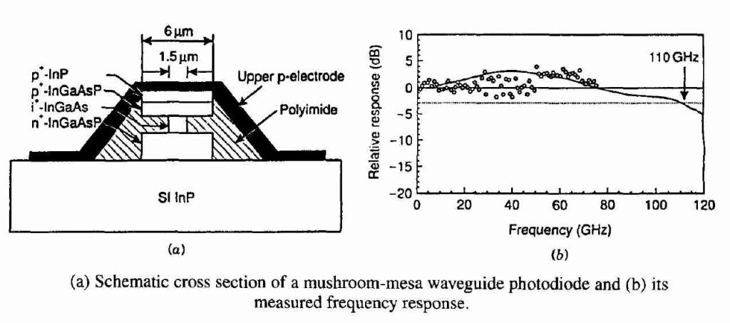
It was measured by using a spectrum analyzer (circles) as well as taking the Fourier transform of the short-pulse response (solid curve). Clearly, waveguide p-i-n photodiodes can provide both a high responsivity and a large bandwidth. Waveguide photodiodes have been used for 40-Gb/s optical receivers and have the potential for operating at bit rates as high as 100 Gb/s.
The performance of waveguide photodiodes can be improved further by adopting an electrode structure designed to support traveling electrical waves with matching impedance to avoid reflections. Such photodiodes are called traveling-wave photodetectors. In a GaAs-based implementation of this idea, a bandwidth of 172 GHz with 45% quantum efficiency was realized in a traveling-wave photodetector designed with a 1-μm-wide waveguide. By 2000, such an InP/InGaAs photodetector exhibited a bandwidth of 310 GHz in the 1.55-μm spectral region.


