The Power of Photodetectors in Optical Fiber Communication
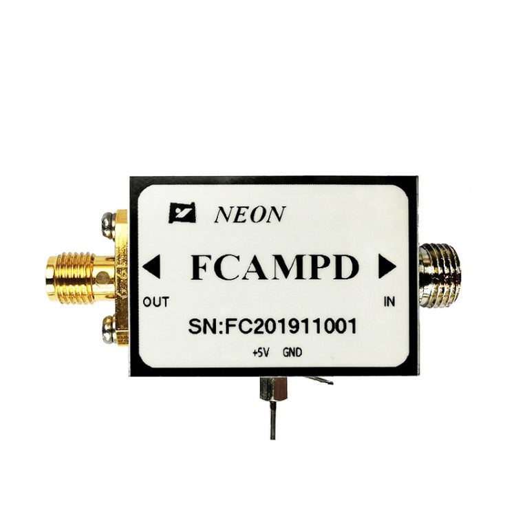
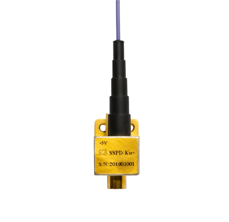
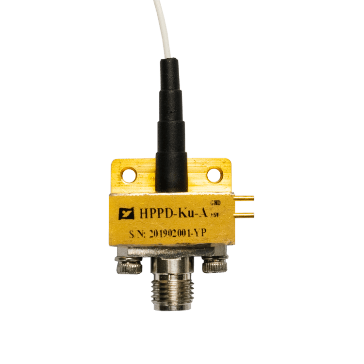
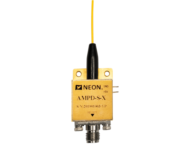
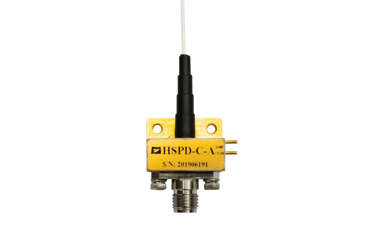
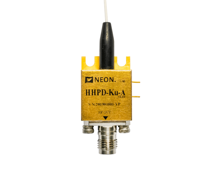
The pulsating lifeblood of modern communication networks courses not through metallic arteries, but through ethereal conduits of glass: optical fibers. These hair-thin filaments convey information encoded in light pulses, traversing vast distances with minimal attenuation and propelling the information age forward. However, the light’s journey culminates not in a nebulous realm of photons, but in the tangible domain of electronics. This transformative act, the conversion of light into electrical signals, lies at the heart of the photodetector in optical fiber communication.
Within this diminutive semiconductor device unfolds a delicate interplay of physics and engineering. Incident photons, bearers of information, interact with the photodetector’s internal structure, triggering a cascade of events that ultimately generate an electrical current. This current, proportional to the light intensity and modulated by the information encoded therein, becomes the conduit for further processing and interpretation.
Types of Photodetectors in Optical Communication
The realm of photodetectors employed in optical communication is not a homogenous landscape. Different architectures, each with its own strengths and limitations, cater to diverse application needs. Here, we delve into the operational principles and key characteristics of four prominent types:
1. p-n Photodiodes
The p-n photodiode, the workhorse of the industry, embodies a minimalistic elegance. Its core lies in the junction of p-type and n-type semiconductor regions, forming a built-in electric field. When light penetrates this junction, it generates electron-hole pairs. The electric field sweeps these pairs apart, resulting in a photocurrent directly proportional to the incident light intensity. This straightforward architecture translates into several advantages:
- Simplicity in fabrication: p-n photodiodes boast a relatively simple manufacturing process, leading to cost-effective production.
- High sensitivity: Despite their basic design, p-n photodiodes exhibit appreciable sensitivity, making them suitable for a wide range of communication applications.
- Good linearity: The relationship between light intensity and photocurrent in p-n devices is highly linear, ensuring faithful reproduction of the information encoded in the light pulses.
However, simplicity comes at a cost. p-n photodiodes are inherently limited by their relatively slow response times and narrow bandwidths, restricting their suitability for high-speed communication scenarios.
2. p-i-n Photodiodes
Building upon the p-n foundation, the p-i-n photodiode introduces an intrinsic (undoped) semiconductor region between the p and n layers. This seemingly subtle addition yields significant benefits:
- Increased absorption area: The intrinsic region expands the light-sensitive volume within the device, leading to enhanced absorption and higher sensitivity compared to p-n counterparts.
- Wider bandwidth: The p-i-n design facilitates faster carrier collection, enabling the device to respond to higher-frequency light pulses and broadening its operational bandwidth.
However, this increased complexity comes with a slight cost increase compared to p-n photodiodes.
3. Avalanche Photodiodes (APDs)
For applications demanding extreme sensitivity, the avalanche photodiode (APD) emerges as a formidable champion. This device incorporates a high electric field within the intrinsic region. When light generates electron-hole pairs, these carriers are accelerated by the intense field, triggering impact ionization. This phenomenon generates additional electron-hole pairs, resulting in an avalanche effect that significantly amplifies the photocurrent.
This amplification grants APDs unmatched sensitivity, making them ideal for low-light conditions or long-distance communication. However, this power comes at a price:
- Increased complexity: The fabrication and operation of APDs require careful control of the electric field and temperature, leading to higher costs and increased susceptibility to noise.
- Limited operating temperature range: APDs exhibit performance degradation at higher temperatures, necessitating stringent thermal management.
4. Metal-Semiconductor-Metal (MSM) Photodetectors
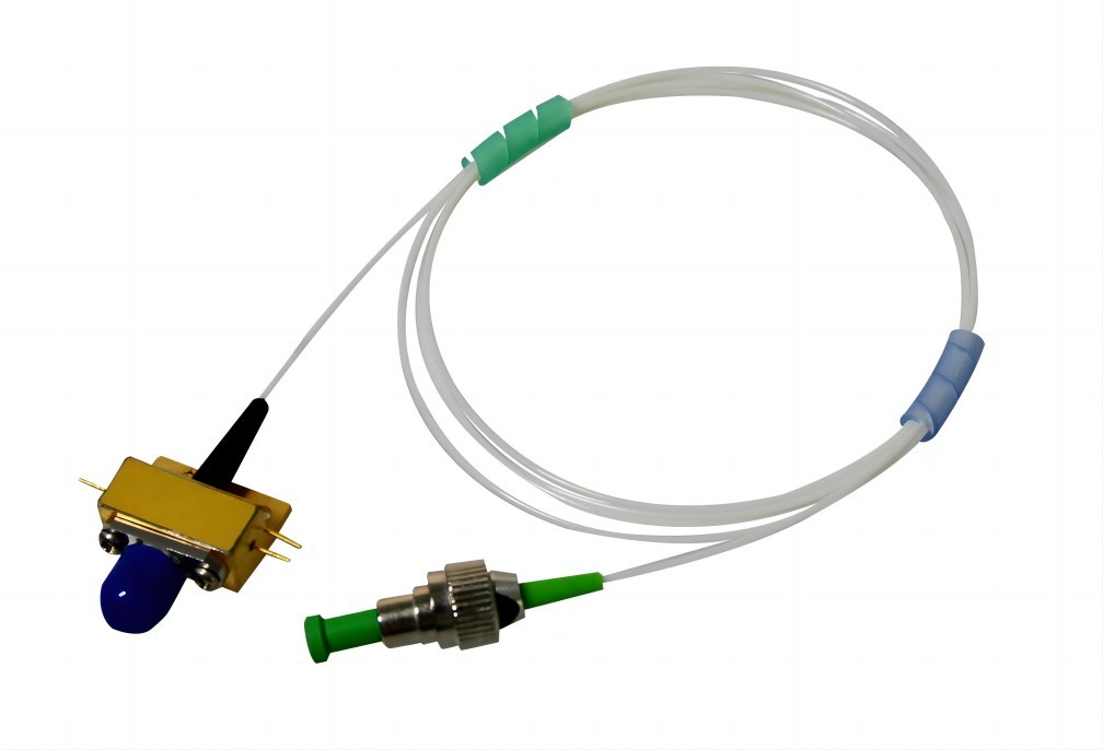
When the focus shifts to high-speed communication, the metal-semiconductor-metal (MSM) photodetector takes the spotlight. This device features two metal electrodes sandwiching a thin semiconductor layer. Light absorption in the semiconductor generates electron-hole pairs, which flow towards the electrodes, creating a photocurrent.
This architecture offers distinct advantages:
- Fast response time: The direct electrode-semiconductor contact minimizes carrier transit times, enabling MSM photodetectors to respond to ultra-fast light pulses with minimal delay.
- Wide bandwidth: The efficient carrier collection also translates into a broader operational bandwidth, making MSMs ideal for high-bit-rate communication.
However, this emphasis on speed comes with a trade-off:
- Lower sensitivity: Compared to other types, MSM photodetectors exhibit inherently lower sensitivity, limiting their suitability for low-light applications.
- Susceptibility to noise: The exposed metal electrodes in MSMs make them more susceptible to electromagnetic interference and other noise sources compared to other photodetectors.
Beyond the Standard: Emerging Trends and Future Visions
The landscape of photodetectors in optical communication is not static. Technological advancements are constantly pushing the boundaries of performance, paving the way for exciting new opportunities. Here, we glimpse into some of these emerging trends:
- Quantum-dot photodetectors: Utilizing nanometer-sized semiconductor particles, these devices offer the potential for ultra-high sensitivity and improved operating temperatures.
- Monolithic integration: Integrating photodetectors directly with other optical components, such as lasers and modulators, promises streamlined system design and enhanced efficiency.
- Silicon photonics: Leveraging mature and cost-effective silicon fabrication technology for on-chip optical circuits, including photodetectors, holds immense promise for large-scale and low-cost optical communication solutions.
Challenges and Considerations
Despite the rapid advancements, several challenges remain:
- Material growth and fabrication: Producing high-quality semiconductor materials and heterostructures with precision is crucial for optimal performance.
- Noise reduction and mitigation: Minimizing noise sources within photodetectors is essential for maintaining signal integrity and ensuring accurate data transmission.
- Packaging and integration: Efficient packaging and integration of photodetectors with other components are vital for real-world implementation and system miniaturization.
Conclusion
The photodetector in optical fiber communication is more than just a device; it is a bridge between the ethereal realm of light and the tangible world of electronics. Understanding its diverse types, emerging trends, and existing challenges is crucial for advancing the frontiers of optical communication and unlocking the full potential of this transformative technology. As we delve deeper into the fascinating world of photodetection, we can expect even greater breakthroughs, pushing the boundaries of communication and propelling us towards a future fueled by light.


