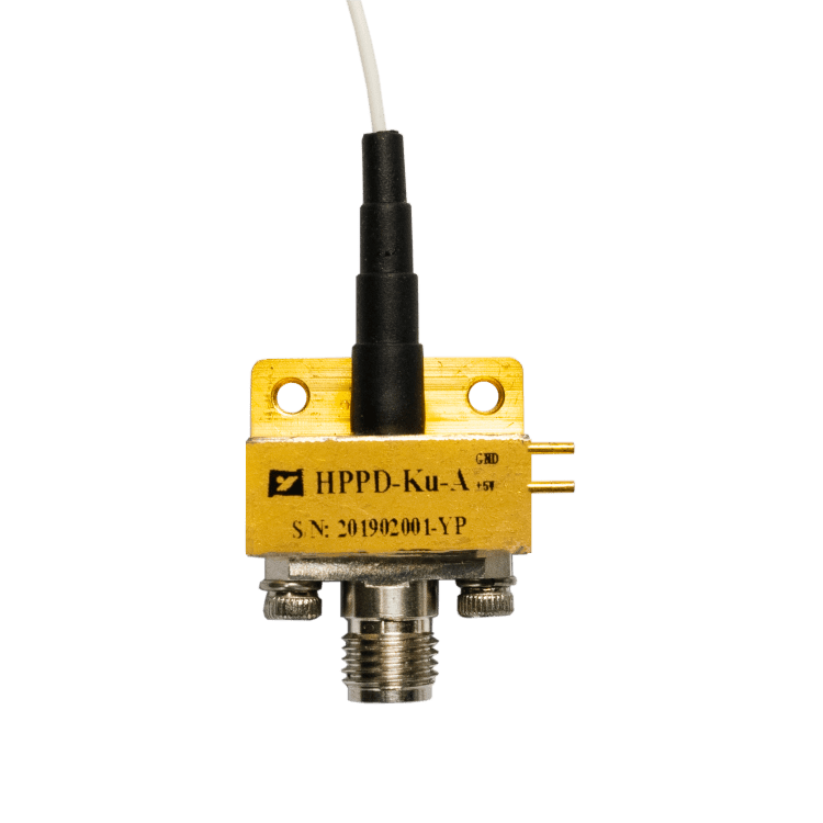
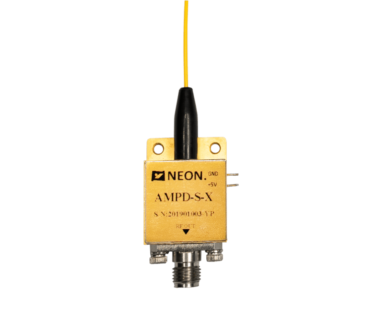
Understanding PIN Photodetectors and Their Role in Optical Communication
PIN photodetectors are vital components in optical communication systems, converting optical signals into electrical signals for further processing. The name “PIN” comes from the three distinct layers of semiconductor material that form the device: the P-type, Intrinsic (I), and N-type layers. These photodetectors offer high sensitivity, fast response times, and the ability to handle a wide range of optical signals, making them indispensable in various applications like fiber-optic communication, environmental monitoring, and medical diagnostics. This article delves into the working principle, structure, manufacturing process, advantages, applications, and the specific use of Gallium Arsenide (GaAs) PIN photodiodes in optical communication.
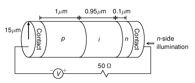
Structure of PIN Photodetectors
The structure of a PIN photodetector is a meticulously engineered assembly of three distinct semiconductor layers: the P-type layer, the intrinsic (I) layer, and the N-type layer. Each layer contributes uniquely to the overall functionality of the device.
- P-Type Layer: The P-type layer is typically very thin compared to the other layers and is used to collect holes (positive charge carriers). This layer is heavily doped to create a high concentration of holes. Its role is critical in ensuring that the holes generated in the I-layer are effectively collected.
- Intrinsic (I) Layer: The intrinsic layer, often called the light-absorbing layer, plays a pivotal role in the photodetector’s function. This layer is usually thick enough to absorb incoming light and generate electron-hole pairs. Unlike the P-type and N-type layers, the intrinsic layer is undoped, which minimizes the presence of free carriers and allows the generated electron-hole pairs to be efficiently separated by the internal electric field.
- N-Type Layer: The N-type layer is similar to the P-type layer in that it is thin and used to collect electrons (negative charge carriers). It is heavily doped with donor impurities to create a high concentration of electrons. The N-type layer completes the electrical circuit, collecting the negative carriers generated in the I-layer.
The thickness and doping concentration of each layer, particularly the I-layer, are key to optimizing the photodetector’s performance, such as its quantum efficiency, frequency response, and sensitivity to different wavelengths of light.
Working Principle of PIN Photodetectors
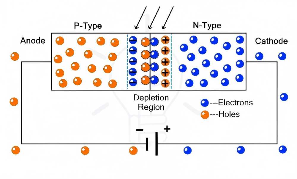
The functioning of a PIN photodetector is based on the photoelectric effect, where photons of light striking the material generate electron-hole pairs that can be separated by an internal electric field, producing a photocurrent. Let’s break down the core steps of how this works:
- Photonic Absorption: When photons with sufficient energy strike the intrinsic (I) layer of the PIN photodetector, they get absorbed. The energy from the photons excites electrons in the material, causing them to move from the valence band to the conduction band, creating electron-hole pairs. The energy of the photons must be higher than the bandgap of the semiconductor for this process to occur.
- Carrier Separation: The intrinsic (I) layer of the PIN photodetector is crucial because it is designed to be nearly free of charge carriers and is wider than the depletion region found in simple PN junctions. When electron-hole pairs are created in this layer, the built-in electric field across the P-I-N junction quickly separates the electrons and holes. The electrons move towards the N-type layer, and the holes drift toward the P-type layer.
- Carrier Collection: Once the electrons and holes are separated, they are collected by the electrodes attached to the P-type and N-type materials. These carriers generate a photocurrent, which is proportional to the intensity of the incoming light. This electrical signal can then be amplified, processed, and transmitted as needed in communication systems.
Manufacturing Process of PIN Photodetectors
The manufacturing of PIN photodetectors is a highly intricate and multi-step process that demands precision and control at every stage. It involves a combination of advanced semiconductor processing techniques and careful material selection to ensure the production of high-quality devices. Below are the key steps involved in manufacturing a typical silicon-based PIN photodetector:
- PECVD Deposition: Plasma-enhanced chemical vapor deposition (PECVD) is used to deposit a layer of silicon dioxide (SiO₂) on a silicon wafer. This layer serves as an insulating layer during photolithography.
- Boron Ion Implantation: A boron ion implant is used to create the P-type layer by introducing boron atoms into the silicon wafer. The implant depth typically reaches around 200 nm, determining the size of the P-type region.
- High-Temperature Annealing: After the implantation, the wafer is subjected to high-temperature annealing (typically around 500°C) to activate the dopants and repair any damage caused during the implantation process. This step ensures that the P-type layer has the desired electrical characteristics.
- Passivation and Metallization: A passivation layer of SiO₂ is deposited to protect the photodetector from contamination and oxidation. A thin metal layer is then deposited on the front of the device to form an electrode. This is followed by the creation of a back electrode, typically formed by Ti/Pd/Ag metal deposition, to complete the device structure.
This intricate fabrication process is essential for optimizing the PIN photodetector’s electrical and optical properties, especially its response time and dark current characteristics.
Advantages of PIN Photodetectors
Compared to conventional photodetectors, such as PN junction photodiodes, PIN photodetectors offer several distinct advantages:
- Wide Frequency Bandwidth: PIN photodetectors can handle a wide frequency range, with some devices capable of operating up to 10 GHz. This makes them suitable for high-speed optical communication systems where high data rates are required.
- High Sensitivity: PIN photodetectors are highly sensitive to light and capable of detecting low light levels. Their ability to convert even weak optical signals into electrical signals makes them indispensable for applications requiring high sensitivity.
- Wide Linear Output Range: These photodetectors exhibit a broad linear response to varying light intensities. This characteristic allows them to work efficiently across a wide range of optical power levels without significant distortion or saturation, which is critical in real-world applications.
- Low Noise: PIN photodetectors typically exhibit low dark current, which helps minimize noise in the signal and enhances the signal-to-noise ratio. This is particularly important for long-distance optical communication, where signal degradation due to noise can lead to errors.
These advantages ensure that PIN photodetectors are well-suited for use in advanced optical communication systems, where reliability and high performance are paramount.
Application Areas of PIN Photodetectors
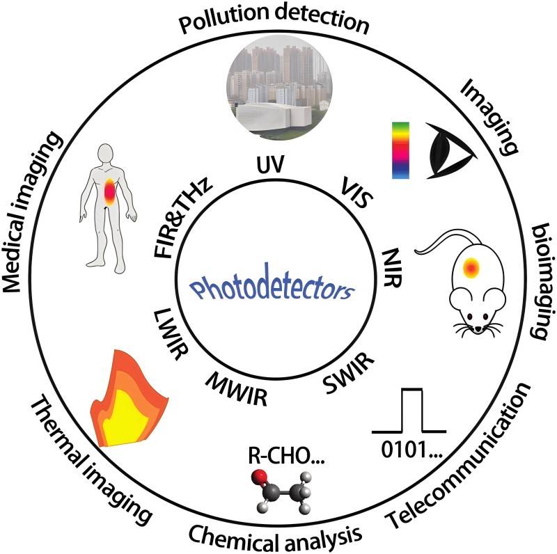
PIN photodetectors find applications in a variety of industries, where their ability to convert light into electrical signals efficiently is essential:
- Optical Communication: In optical communication systems, PIN photodetectors are used as receivers that convert the light pulses transmitted through fiber-optic cables into electrical signals. Their high sensitivity and fast response times make them ideal for modern telecommunications, enabling high-speed data transmission over long distances.
- Environmental Monitoring: PIN photodetectors are employed in environmental monitoring applications, such as detecting atmospheric pollution or measuring light scattering for weather forecasting. Their ability to detect a wide range of wavelengths makes them versatile for different types of environmental sensors.
- Medical Devices: In medical imaging, particularly in devices like CT scanners and X-ray machines, PIN photodetectors are used to detect X-rays and convert them into signals that can be processed to form images. Their fast response time and low noise make them suitable for high-precision medical diagnostics.
High Speed GaAs PIN Photodiode with Advanced Material
While silicon is the most commonly used material for PIN photodetectors, Gallium Arsenide (GaAs) is increasingly being used for high-performance applications, especially in optical communication. GaAs photodiodes have several advantages:
- Material Properties: GaAs have a direct bandgap, which allows them to efficiently absorb photons and convert them into electron-hole pairs. This characteristic makes GaAs PIN photodiodes more sensitive and faster than silicon-based devices.
- Higher Speed and Efficiency: GaAs-based PIN photodiodes can operate at higher speeds and are less sensitive to temperature variations compared to silicon devices. This makes them ideal for high-speed optical communication systems.
- Applications: GaAs PIN photodiodes are used in advanced optical communication networks, where high bandwidth and fast data transmission are crucial. They are also used in space communication and military applications, where their high performance and durability are required.
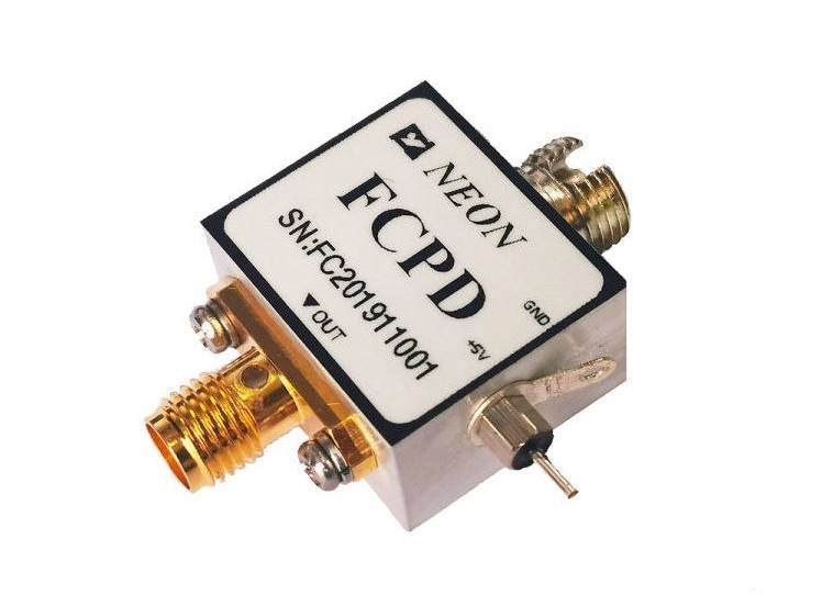
PIN photodetectors are fundamental components in modern optical communication systems, offering high sensitivity, fast response times, and wide bandwidth. Their intricate structure, combined with advanced manufacturing techniques, ensures that they can meet the demands of a wide range of applications, from telecommunications to environmental monitoring and medical diagnostics. GaAs-based PIN photodiodes, in particular, are paving the way for even faster and more efficient communication technologies. As optical communication continues to evolve, PIN photodetectors will remain at the heart of these advancements, ensuring reliable, high-speed data transmission for the future.


